Making PCBs

Why Bother?#
So, why would anyone bother making PCBs at home? The truth is that not many people do any more. In the year 2025, we have the ability to order high quality PCBs form China for next to nothing. If you just want a high quality board and you don’t mind waiting a week or two, these are a great option.
I however, don’t like to wait. I want a PCB in my hands the same day I finish the design.
On the other side of the argument, why bother with a PCB at all, just use some perfboard or a breadboard. I don’t stock though hole components any more, and before I had the CNC, I really didn’t feel like drilling loads of holes by hand.
A bit of History#
Printed Circuit Boards used to be something that you had to know how to make yourself if you wanted to do anything serious with electronics since about the ’80s. Before then, people mostly relied on point to point wiring and wire wrapping.
Paint it Black#
Magazines used to have scale prints of hand drawn circuit boards that you could photocopy and transfer onto the copper clad.
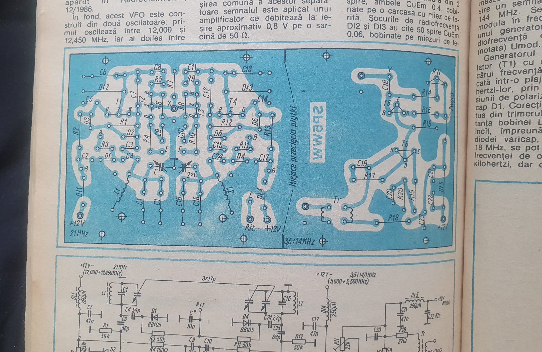
If you wanted a custom design, you could get stencils for common footprints. You would lay them out, connect the pins with a pain marker and etch the board.
All you needed was the copper clad, some paint (nail polish works well), something to drill the holes, and an acid to etch the copper away.
I have used this technique as a young kid to etch my own PCBs, and so did my father before me.
Lasers are Cool#
Later on, I couldn’t tell you exactly when, the toner transfer method became popular. Laser printers don’t use ink, they use a plastic powder we call toner. Is basically the same thing used in powder coating.
This improved on the previous method by allowing much higher precision as well as faster though put. Toner transfer is still popular today, as the barrier to entry is quite small, but it can be fiddly and doesn’t always produce the best results.
Photolithography#
Around the late ’00s, I started seeing people using photolithography. There are two main types, pre-coated PCB clad and dry film lamination. The pre-coated stuff is good and reliable, but you only get one shot and its pretty expensive. You also don’t get many options for thickness and dielectric. Dry film photoresist is a UV curable resin gel, that you laminate onto bare copper clad with a bit of heat.
Regardless of which one you use, the process is the same. You create a mask, that lets light though the sections you want exposed and blocks it elsewhere. After aligning the mask carefully, you exposed the board under a UV lamp. You can then peel back the protective film and use a mid basic solution to develop the cured resin. Any uncured resin will wash away, leaving you with a film that will protect you features from being etched.
This process is more reliable than the toner transfer, though at the expense of involving way more specialised equipment. Another big benefit of this method is that you can now easily align 2 masks to produce 2 layer boards. Furthermore, the photoresist film can act as a “poor-man’s” solder mask.
The Future is Now#
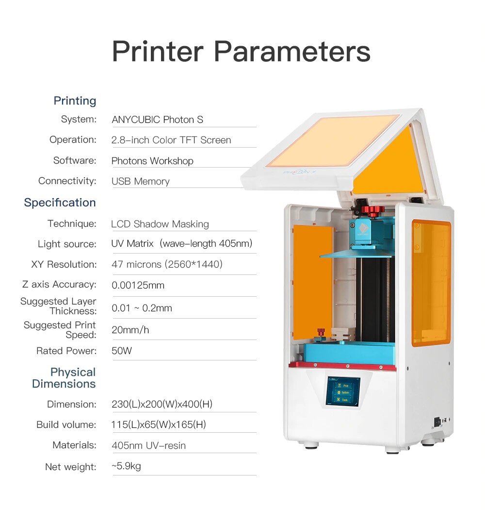 Thanks to some patents expiring, we now have access to really cheap, high resolution SLA 3D printers. I got mine refurbished for £100.
Now we don’t need to bother with printing masks on transparency. You just convert the Gerbers to a format the printer can understand and we are done.
Thanks to some patents expiring, we now have access to really cheap, high resolution SLA 3D printers. I got mine refurbished for £100.
Now we don’t need to bother with printing masks on transparency. You just convert the Gerbers to a format the printer can understand and we are done.
If you don’t plan on using it for 3D printing, you can even take the glass of the LCD to improve the sharpness of the image.
CNC Milling#
You don’t need a CNC mill/router to make PCBs, but it sure helps. Some people even skip the whole etching process and just use the CNC mill to cut around all the traces. This is called isolation routing. Some manufacturers even sell dedicated PCB milling machines.
I can understand the appeal, no chemicals, one machine. The macro timelapses over up beat music are mesmerising. I have tried it, and I don’t like it. Too much noise, for too long, and alignment is a faf.
I do use my mill for drilling whole and routing the edge outline, but that is it.
Lasers Two, Electric Boogaloo#
Another method worth considering if you have a laser cutter is to use it to ablate away a thin layer of paint on top of the copper. I have yet to try this method, but I can imagine it being quite good.
The future#
There are some methods that haven’t yet become main stream, but may do in the future. I will run though as many as I can remember.
- Etching the copper directly with a fibre laser
- Direct to garment resin printers (t-shit printers)
- Metal 3D printing
- Metal vapour deposition (used to make touchscreen digitisers)
- Conductive ink printing
Most of these require machines that are just too expensive right now, but that was also the case for CNC mills and SLA printers less than a decade ago.
My Process#
This is my full process as of 2025.
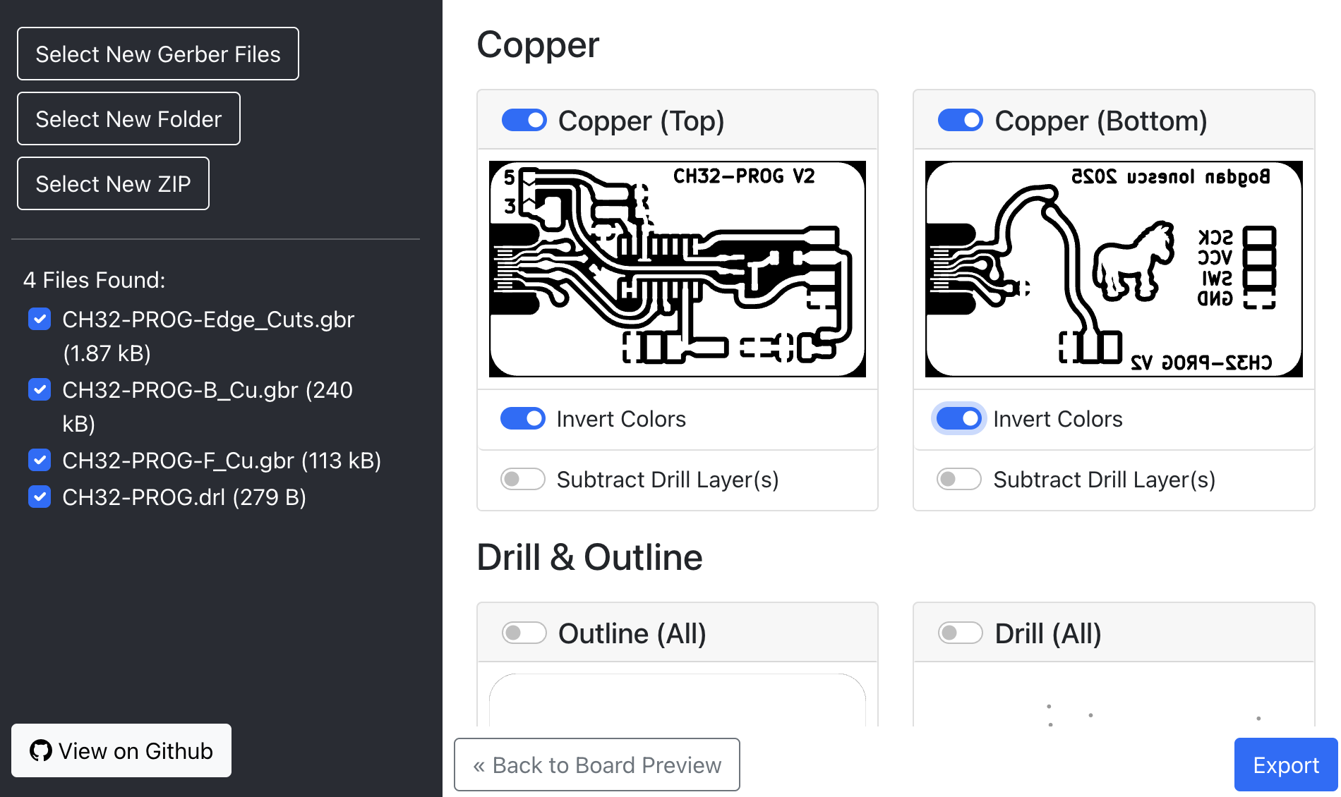
Design#
I design all of my circuits in KiCad, both professionally as well as for personal projects.
Here are my go to parameters:
- 0.3mm traces
- 0.5mm clearance
- 1mm vias with 0.5mm holes
I can achieve much better results than this, and I often need to, but these are very safe parameters for my process. Even if I need finer details, I tend to keep those to an isolated area and loosen the requirements for the rest of the board.
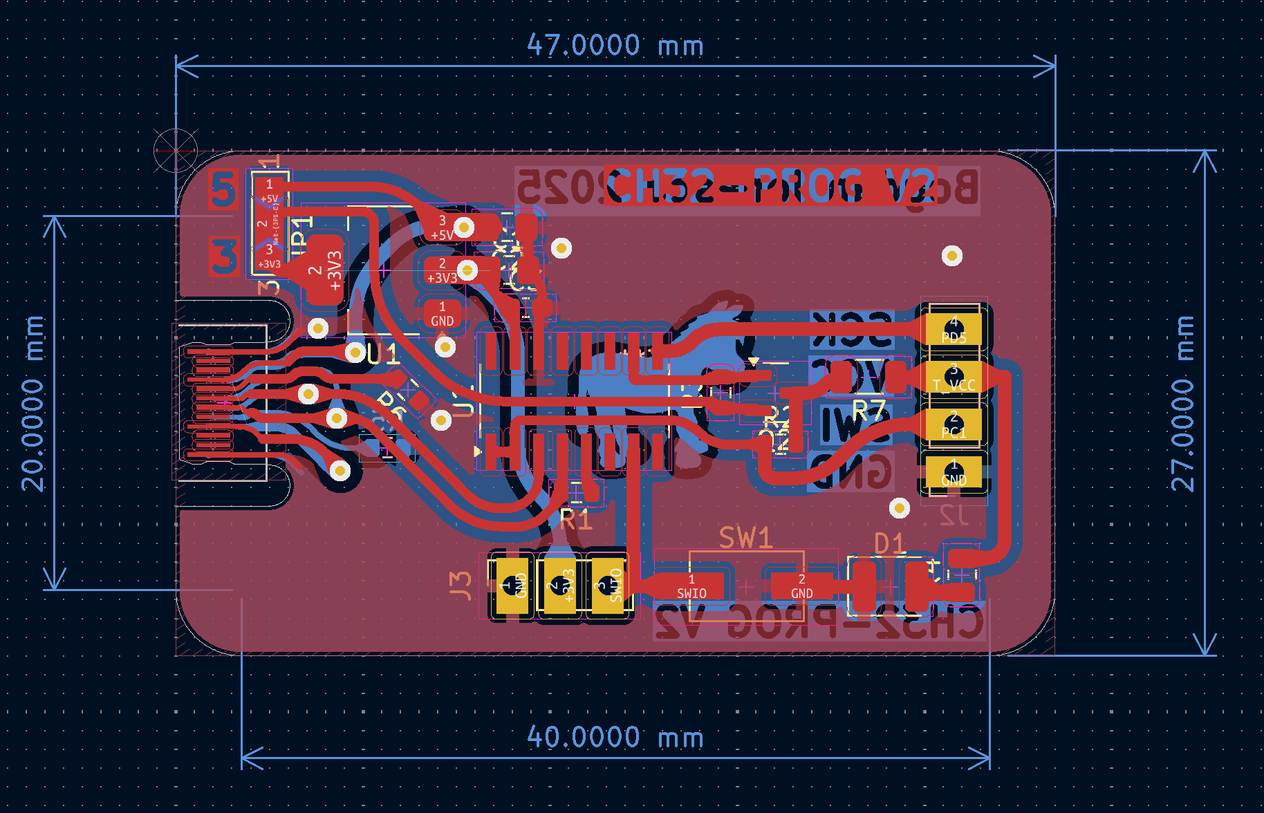
I like to keep my drill place origin at a point that I can easily align to. The round traces and teardrops are not necessary, I don’t tend to use them too much and they make the design harder to edit. I also try to keep my though whole pads quite big, they just minimise the chance of pads lifting.
Once I’m happy with the design, I just export the Gerbers and drill files like I would for any other manufacturer.
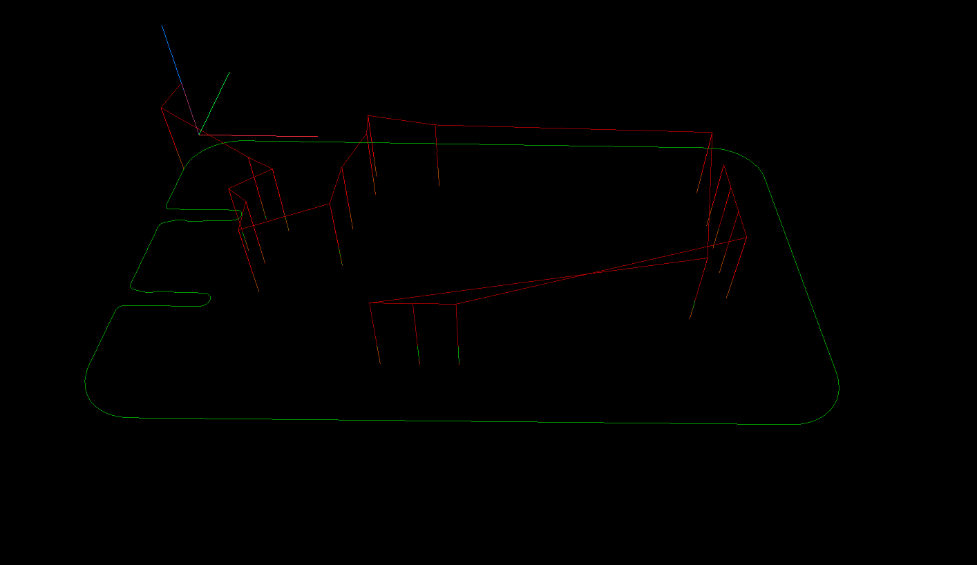
Tool Paths#
This whole section is optional, but I already have a few milling machines so I let the robot cut the board.
I have wrote my own set of FastPCBTools to turn the exported files into G-Code.`
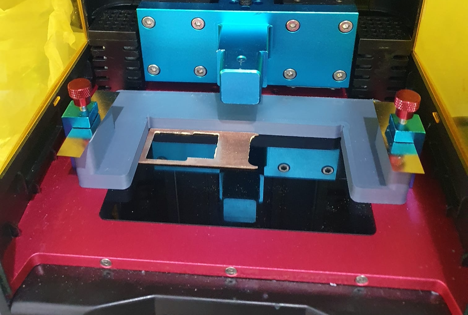
Machining#
I built the first version of CNC mill out of scrap from the university workshop. I have since upgraded it many times. The spindle is powered by a 1,000W Server PSU and it can go to about 15,000rpm, but I rarely run it above 9k as its quite loud.
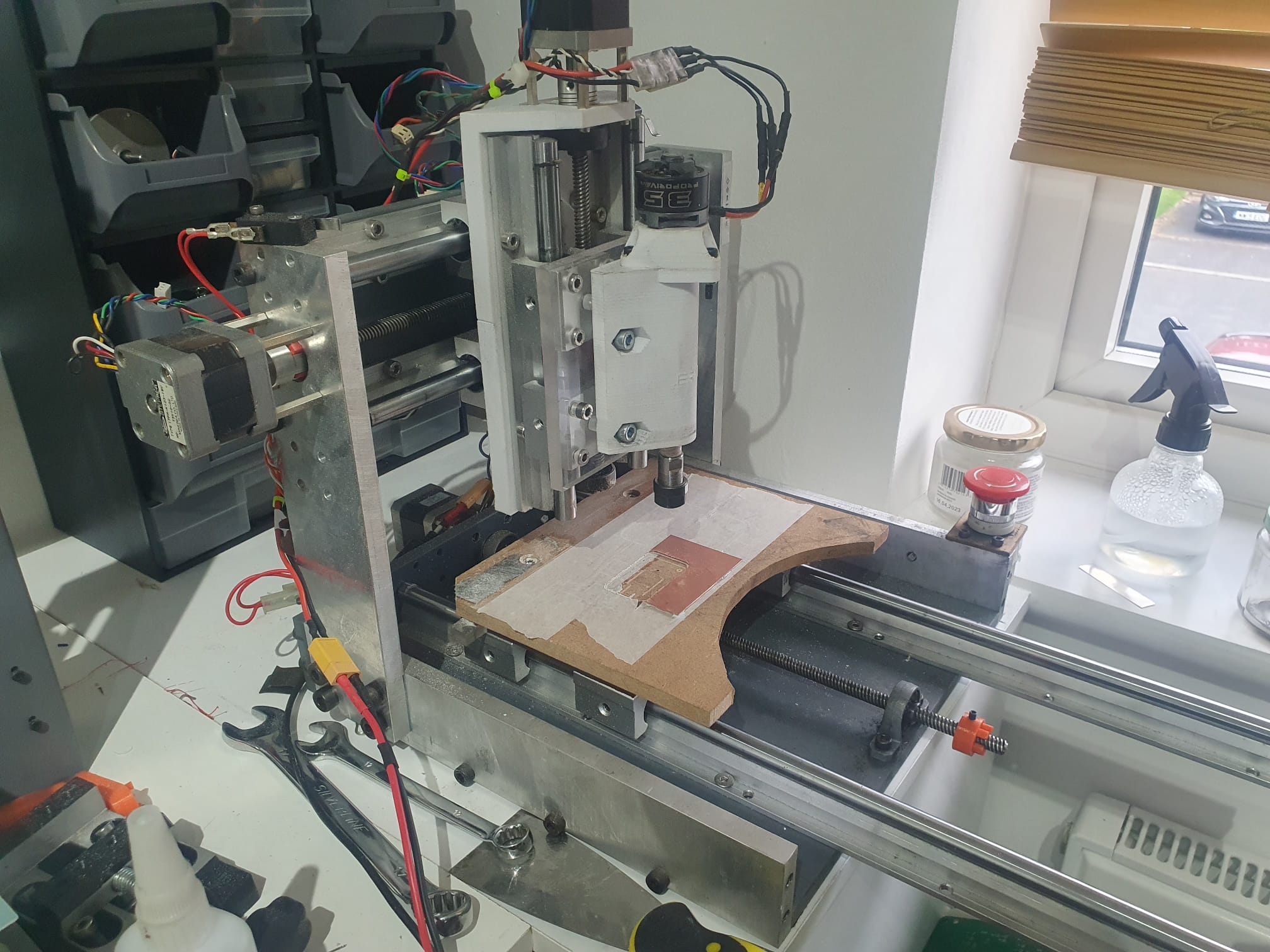
I use masking tape on both the MDF spoilboard and the back of the copper clad. I then apply superglue to one side and stick to down as close to square as I can.
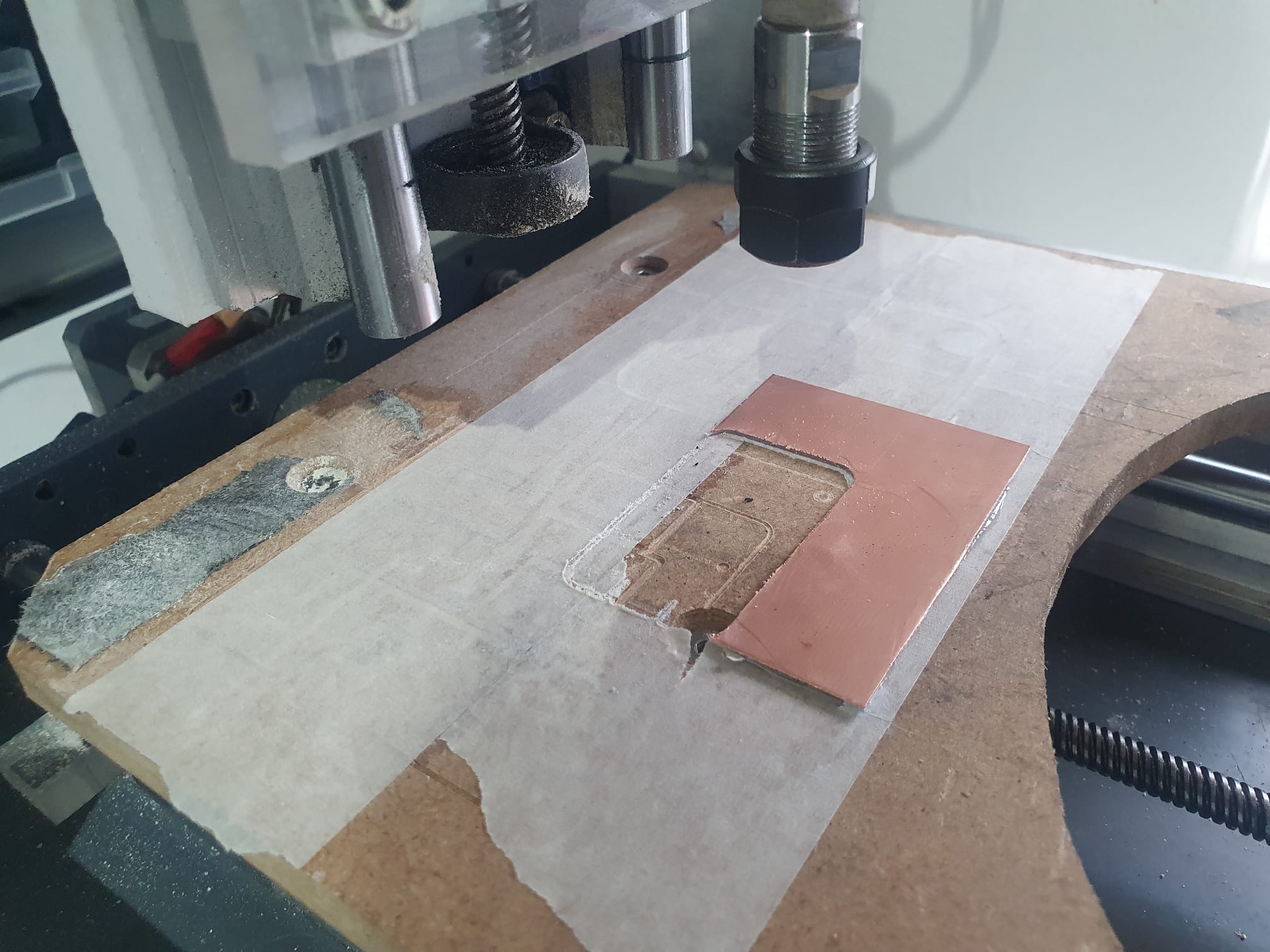
If anyone cares for feeds and speeds, I run everything at 9,000rpm 50mm/s. I use a 1.0mm carbide burr endmill for the edge cuts.
Plotting#
To turn the Gerbers into something that the resin printer can understand, I use a lovely web tool called photonic-etcher.
For my film, 100s exposure seems to work very well, though for finer details, I tend to underexpose.
Laminating#
I use a cheap laminator and pass the copper clad twice on each side between a folded piece of paper. It’s crucial that the surface is clean and no moisture is left in the vias. You will get bubbles otherwise.
Exposure#
I use a 3D printed fence to align the board.
Once both sides are exposed, I peel of the protective foil and we are ready to develop.
Developing#
This is the only activity I do where I can be called a developer, though, the Calcium Carbonate solution is doing most of the work. I am sure there is an optimal solution concentration, I just use a sprinkle in about 500ml of water. Too weak, and it will take too long, too strong and the resin will start coming off the board.
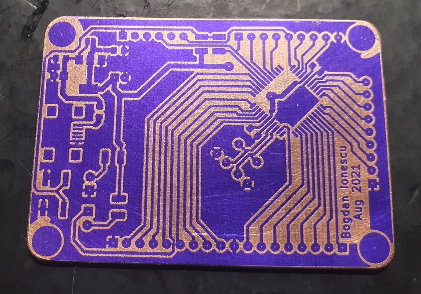
I use a dedicated toothbrush to get in between the traces. I’m not sure how much it helps, but it keeps me busy. If the traces are coming off, its not your scrubbing, the lamination wasn’t good enough. Better to catch it now, before it goes into the Ferric Chloride. If there are any little broken traces or spots, I pain on a bit of nail polish with a very fine brush.
Etching#
Not much to say about etching. Be careful, it stains like nothing else. Use gloves and safety goggles. Don’t use your nice tweezers, unless they are titanium. It can take anywhere from 5-20 minutes to etch though. You can’t leave it in too long.
Soldermask or tinning#
If you want to be fancy, you can add another layer of photoresist, develop it and then bake it to get something resembling soldermask. You can buy the real thing online, but its pretty pricey compared to the normal kind.
Most of the time, I don’t bother. I use a tinning solutions to add a little but of durability and corrosion resistance, but only if the board is going to see any sort of real use. If it’s just a quick prototype, I might just leave the copper bare.
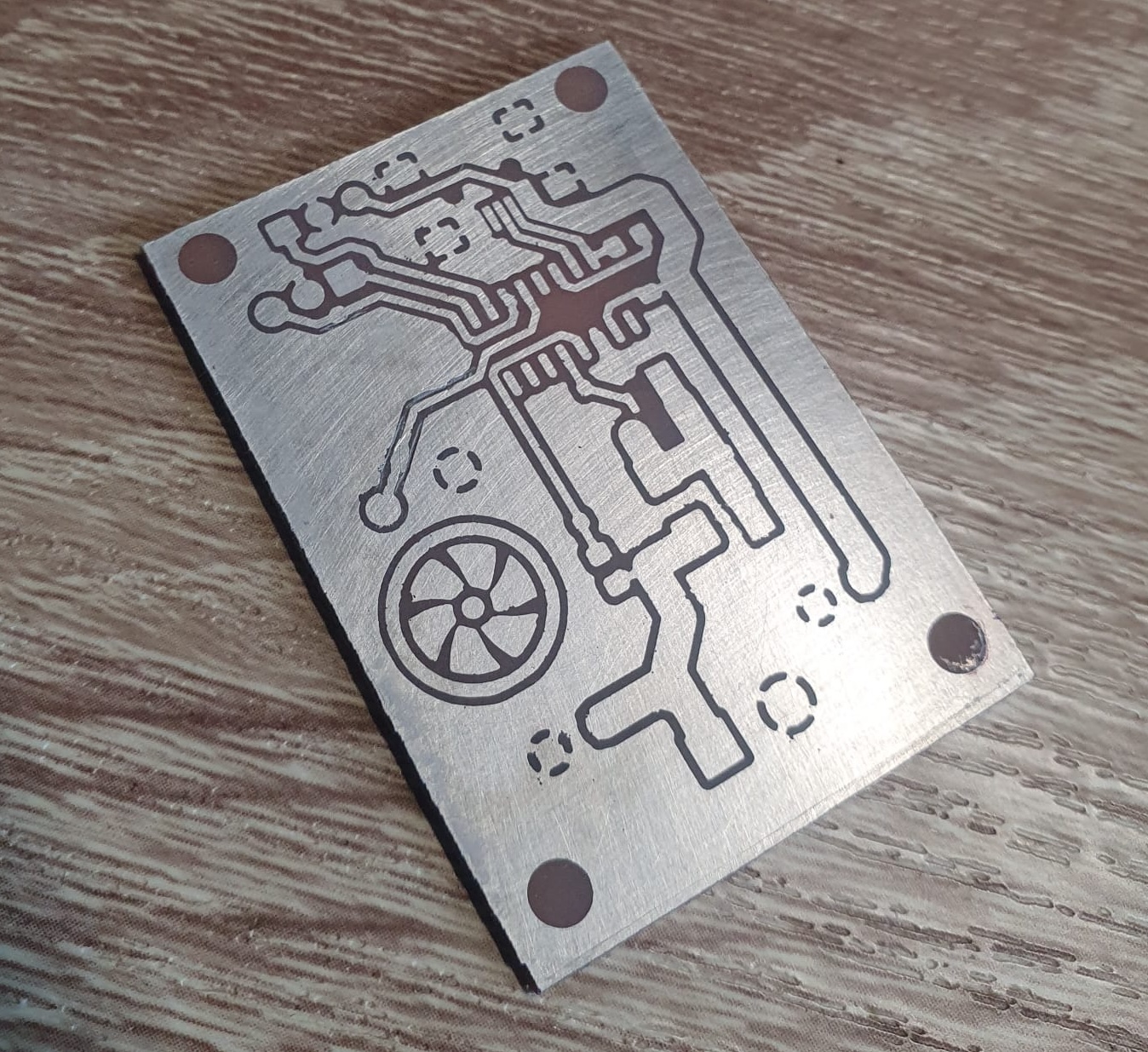
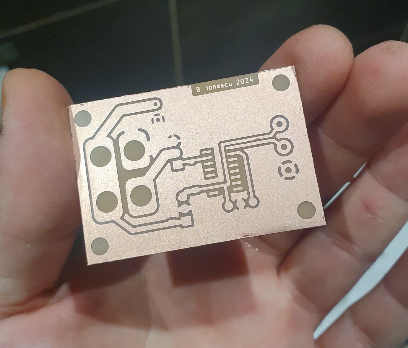
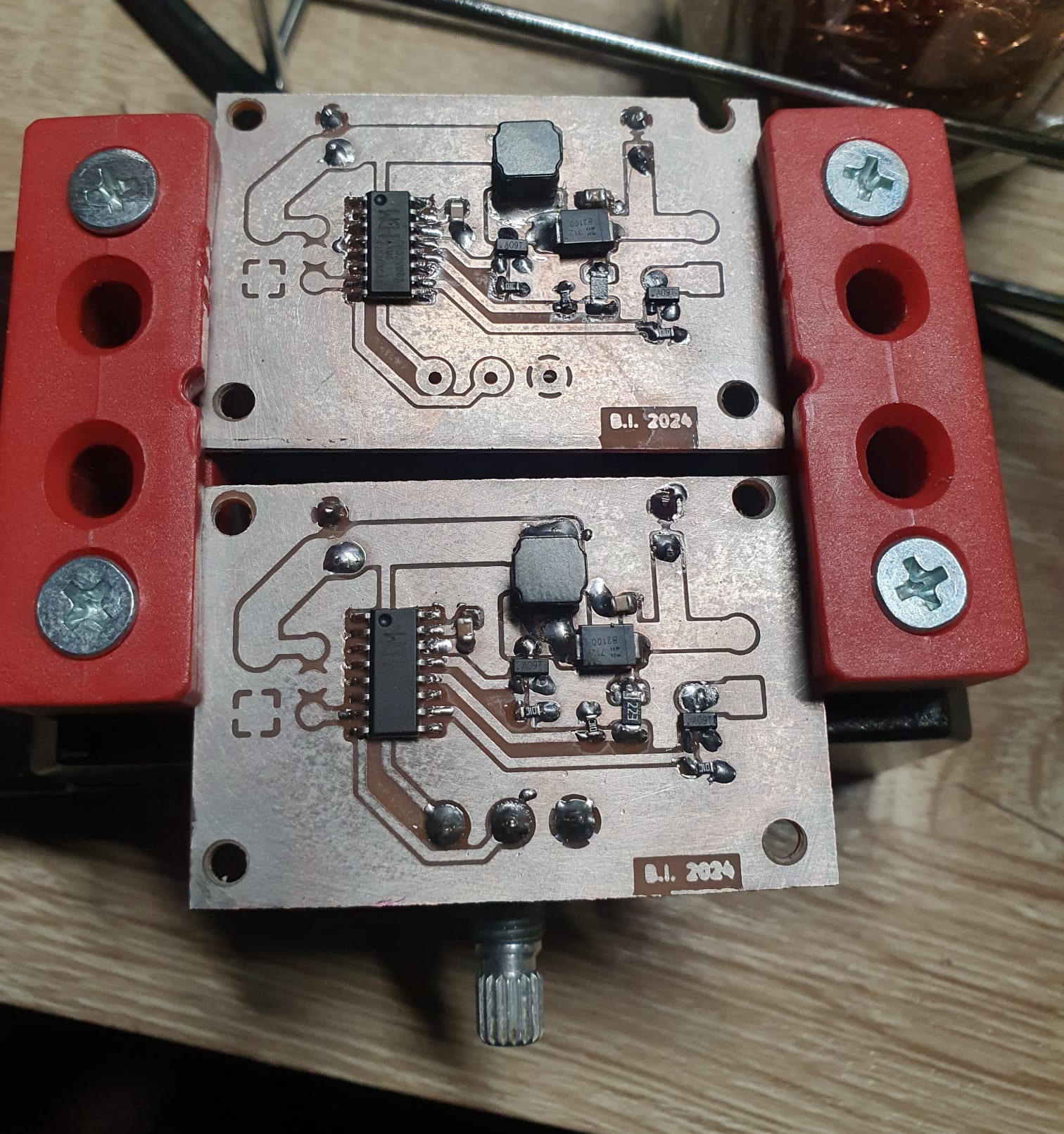
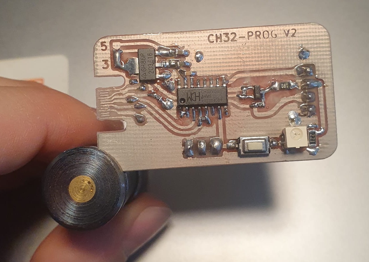
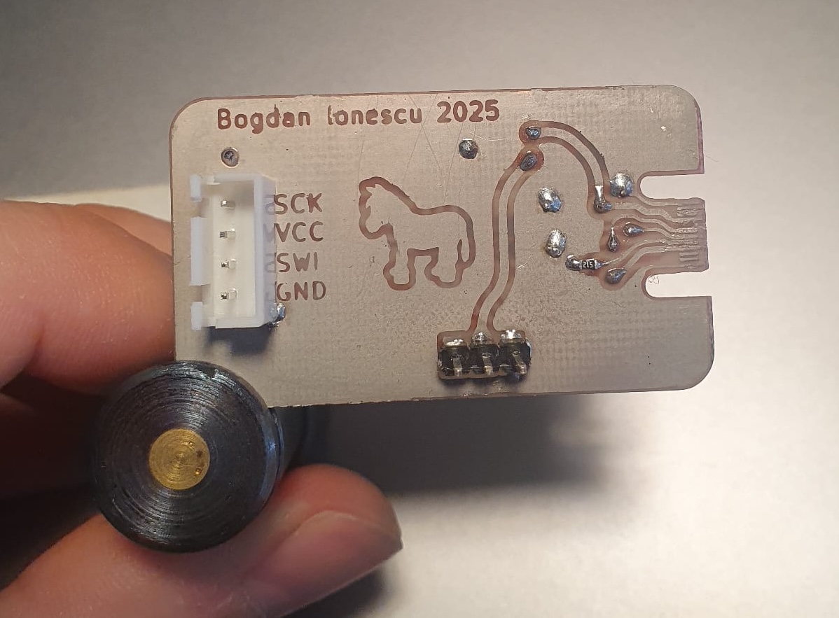
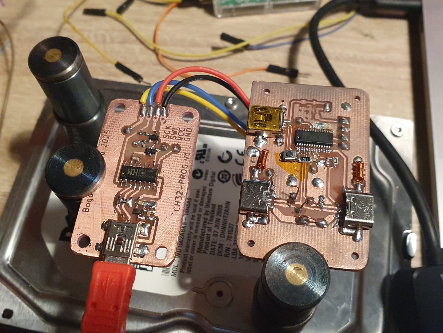
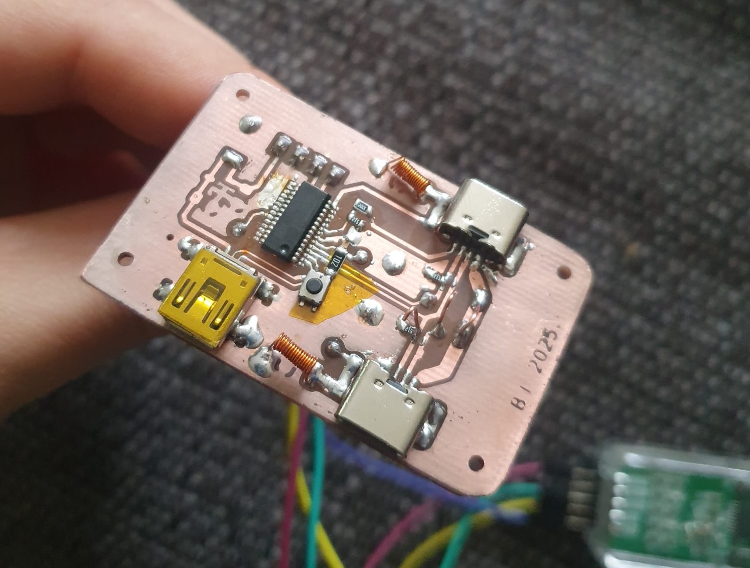
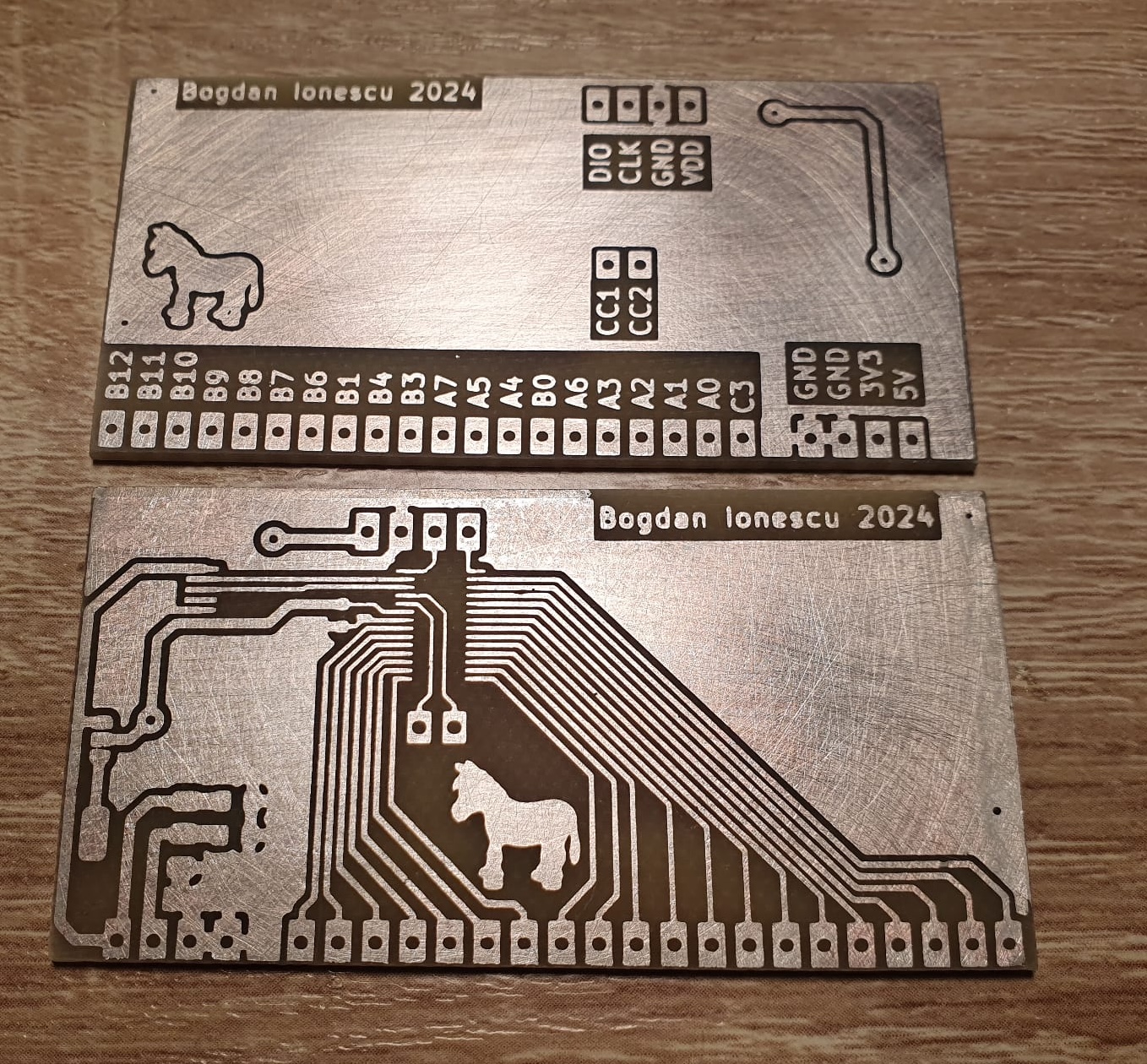
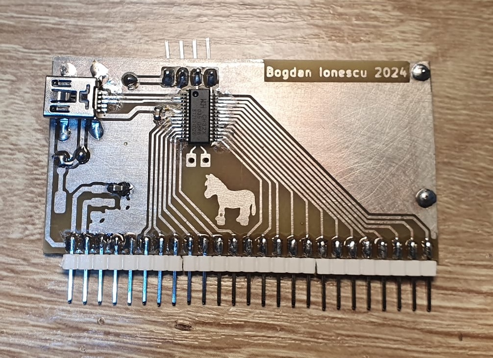
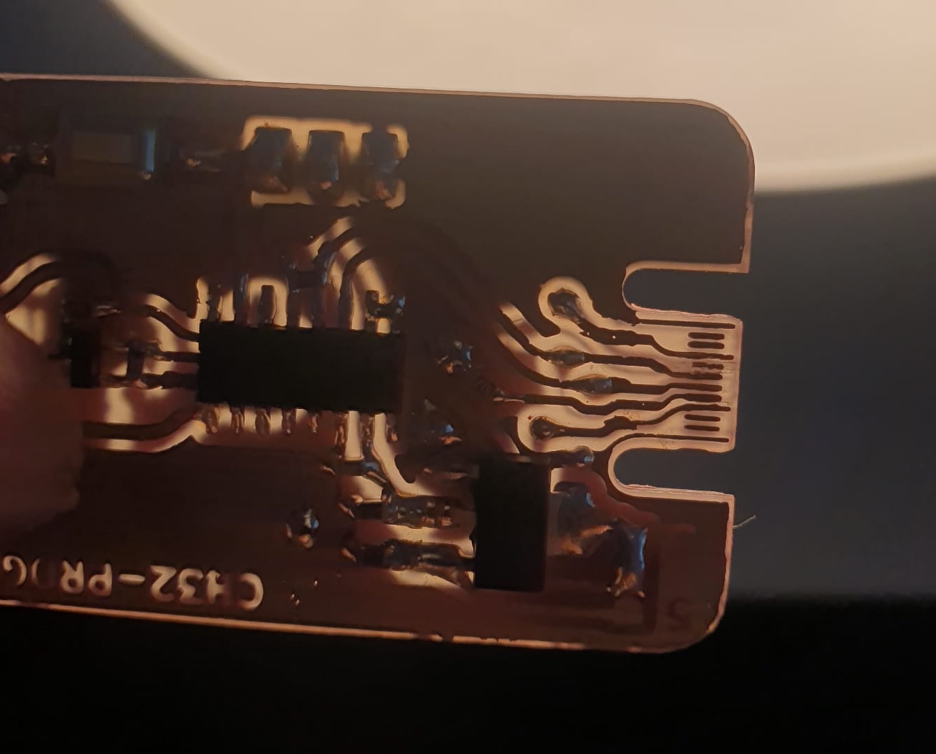
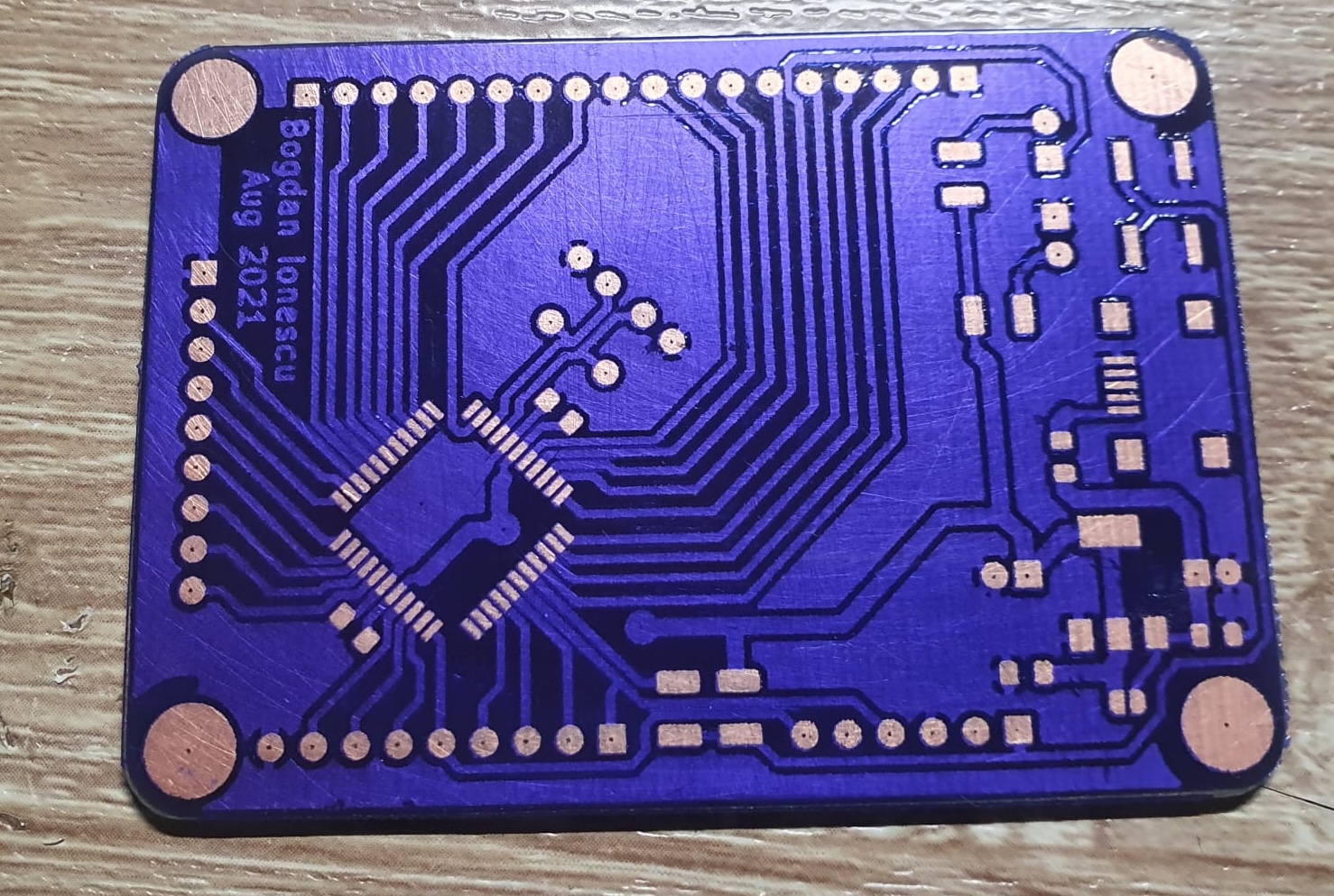
Gallery#
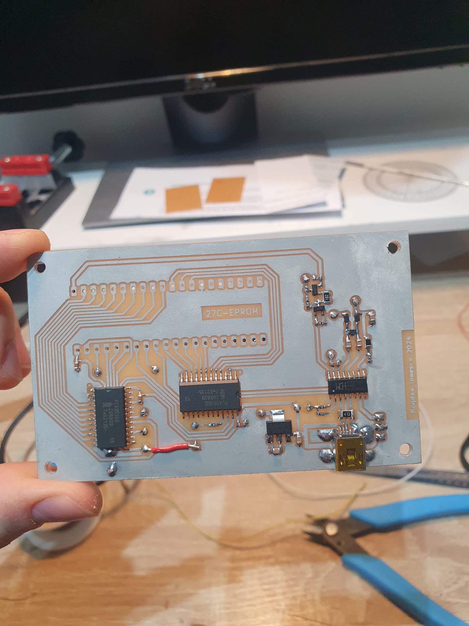
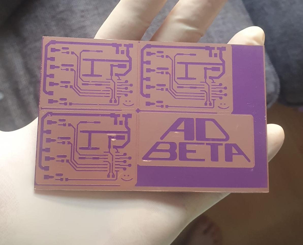
Finally, here are some PCBs I made with this technique at various stages of progress. I make about 2 PCBs a month, so these are only the ones I bothered taking pictures of.